请完成以下验证码
|
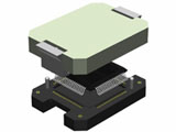
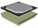
Any package style: ceramic & plastic BGA, CSP, LGA, CGA, PSGA, MLF/QFN,QFP, SOIC, and other standard packages, custom packages or bare die
Inductance: less than 2nH
-1dB bandwidth: >14GHz for compression style; 3GHz for SMD style
available for any chip size and grid pattern
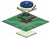
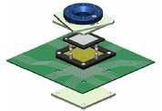
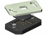
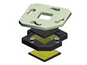
Same PCB layout as the IC (no holes required for SMD socket)
Minimal keepout area of 6mm beyond the IC’s periphery
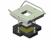
Raised SMD style for lifting socket over adjacent components
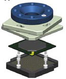
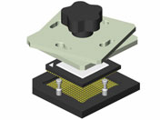
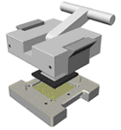
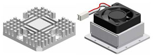
Low profile socket (standard Twist Lock is less than 10mm high with IC)
Contact force: max 40 grams per contact; lower forces available
Semi-custom design = lower cost and tailored to your needs