How to create a new PSoC project ?
Step 1: Create a Project
In PSoC Designer 5.2, you can create a new project with the following steps.
Click the File menu and select New Project.
Choose any desired name for the project and click OK.
Select View Catalog to select the target device. Click Select when the device has been selected.
Select your language and click OK and PSoC Designer will create your project.
Step 2: Choose a Base Device to Work With
The device editor that powers the Chip-Level view shows you the resources available on your chosen PSoC device and allows you to configure and route those resources. After you have created a project, step two is to choose a device.
Click the View catalog button.
In the Select Base Part dialog, choose the part used in your kit. The CY3210-PSoCEval1 uses the CY8C29466-24PXI. Consult your kit document for the proper device for your kit.
Click Select.
Choose Generate ‘Main’ file using C.
Click OK.
Your project opens in the Device Editor Chip-Level view. The default view has secondary windows that show all kinds of information about your project. You can move, resize, close, and arrange all of these secondary windows to suit your working preferences. The View menu contains the available windows.
Step 3: Choose and Configure User Modules
This project divides the output of a potentiometer into three regions. An LED will be off, on, or blinking depending on which of the three ranges the voltage read from the potentiometer is in. The user modules required for this project are:
PGA -A programmable gain amplifier is used to buffer the input from the potentiometer.
ADCINC - An incremental ADC is used to convert the analog input from the potentiometer to a digital value that you can use for the program logic.
Timer8 -An 8-bit timer is used to blink the LED periodically.
Global Resources
Global resources are those shared by all user modules in a particular configuration. The IDE Guide (Help > Documentation) contains a complete reference on the effect of each of the Global Resources.
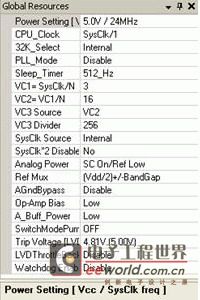
Set the CPU Clock to SysClk/1. Since you left the Power Settings at its default of 5 V operation and a SysClk of 24 Mhz, the CPU will also run at 24 Mhz.
Set the VC1 clock to SysClk/3.
Set the VC2 clock to VC1/16.
Set the VC3 source to VC2 and the VC3 Divider to 256.
PGA
In the User Module Catalog (View > User Module Catalog), double click to expand the Amplifiers folder.
Right-click PGA and select Place. The PGA is placed in the first available analog block. The default placement of the user module is sufficient for this user module.
Select the PGA user module in the Application Explorer.
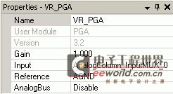
In the Properties window (View > Properties Window) for PGA_1, change the name of the user module to VR_PGA. Note that the user module name in the Chip-Level view updates with the new name. Right click in an open area of the Interconnect view and select Zoom In to get a close up view of the resources. Press [Alt] and click the mouse to pan the window. Right click again and select Original View to restore the original view.
Set the Gain for VR_PGA to 1.000. The PGA is used to buffer the input of the potentiometer, so the Gain is 1.
Set the Input to AnalogColumn_InputMUX_0. The input for the PGA will come from the potentiometer routed from a pin to the AnalogColumn_InputMUX_0. By default, the AnalogColumn_InputMUX_0 is routed from P0[1]. You can click the mux and select one of four pins, but the default is works for this purpose.
For the VR_PGA Reference, select analog ground AGND. For Analog Bus, choose Disable.
Click Port_0_1 in the interconnect view.
Change the name to VR_IN and click OK.
ADCINC
There are a large number of ADCs available. When choosing an ADC for your own application, consult the ADC Selection Guide (there is a link to it at the beginning of each of the ADC data sheets). This project will use the ADNCINC.
Double click to expand the ADCs folder. Double click to expand the ADCINC folder.
Right click the Single Stage Modulator and select Place.
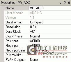
In the Properties Window, change the name of the user module to VR_ADC.
Select Unsigned for the Data Format.
For Resolution, select 8 Bit.
For Data Clock, select VC1.
For PosInput, select ACB00.
This should have connect the output of the VR_PGA GAIN block to the PosInput of the VR_ADC. Check the diagram to make sure that there is a line connecting them. If you are using a chip that has a different configuration of analog blocks than the CY8C29466-24PXI used in the example, choose the block that contains the VR_PGA GAIN block in place of ACB00.
Set the NegInput to ACB00 and the NegInput Gain to Disconnected.
This sets the ADC to use a single ended input.
For PWM Output, select None.
Timer8
The 8-bit timer is used to flash the LED periodically. It uses the interrupt generated by the timer to toggle the LED.
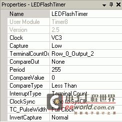
Place a Timer8 user module and rename it LEDFlashTimer.
Set the Clock to VC3.
Set Capture to LOW.
Set TerminalCountOut to Row_0_Output_2. You will route the Terminal Count output to a pin so you can get some practice routing resources in PSoC Designer. You will connect to pin to an LED and set the Drive mode on the pin so that it will flash the LED for a single click cycle every time the timer reaches terminal count.
Set CompareOut to None
Set the Period to 250. The flash rate of the LED will be 1/4 second (24 Mhz / 3 (VC1) / 16 (VC2) / 250 (VC3 Divider) / 250 (Period)). The timer will hit terminal count 8 times per second and each of these terminal counts toggles the LED. The other example project uses the SleepTimer user module rather than the Timer8. The SleepTimer is configurable down to 1 Hz without using the clock dividers. The Timer8 was used in this example to show routing of a user module output to a pin. The same technique can be used o route the output of one user module to the input of another.
Set the CompareValue to 0
Set the CompareType to Less Than
Set the InterruptType to Terminal Count
Set the ClockSync to Sync to SysClk.
Step 4: Connect the User Modules
Each user module has inputs and outputs that can be routed to other user modules and to pins. The output of the VR_PGA user module was routed to the VR_ADC user module in the parameter selection, so to practice routing, you will route the output of the LEDFlashTimer TerminalCountOut to a pin so we can use the signal to flash a LED when the counter reaches terminal count. The main LED from the project will be attached to P0[0] (port 0, bit 0), and the potentiometer input is on P0[1], so you will route this signal to P0[2]. You’ve already routed the TerminalCountOut to row 0 output 2 in the LEDFlashTimer properties.
Locate the RO0[2] (Row_0_Output_2) line in the interconnect view. It is the blue horizontal line that your LEDFlashTimer is attached to.
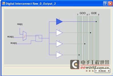
Click the digital interconnect box on the right end of the Row_0_Output_2 line.
In the Digital Interconnect dialog, click the top triangle (Row_0_Output_2_Drive_0) and select GlobalOutEven_2.
Click Close.
In the Pinout Window (View > Pinout) click to expand P0[2].
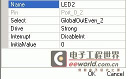
Change the Name to LED2.
Set the Select to GlobalOutEven_2.
Set the Drive to Strong.
Click to expand P0[0] (the other pin that will have an LED attached)
Change the Name to LED1
Set the Drive to Strong.
Click to expand P0[1] and verify that it is named VR_IN and ensure that Select is set to accept AnalogInput .
In the Interconnect view, there is now a line from the TerminalCountOut of the LEDFlashTimer to RO0[2], then to GlobalOutEven_2, and finally to Port_0_2. You have successfully routed the terminal count of your timer user module to a pin and configured the pins for the inputs and outputs attached to them.
Step 5: Write Firmware
The first step in writing the firmware is generating the application. Generating the application creates all of the source files, library files, and headers that are needed to begin writing the firmware. The APIs generated for each of the user modules you have selected are detailed in the user module data sheets associated with each of the user modules.
From the Build menu, select Generate/Build Project.
In the Application Explorer, double click to expand your project folder.
Under the Source Files folder, double click main.c.
Copy and paste the following code into main.c. Replace the entire contents of main.c with this text.
//----------------------------------------------------------------------------
// C main line
//----------------------------------------------------------------------------
#include // part specific constants and macros
// PSoC API definitions for all User Modules
#include \"PSoCAPI.h\"
#pragma interrupt_handler LEDFlashTimer_ISR_C
// Write the interrupt handler for the Flash Timer in C.
#define LED1_PORT PRT0DR
//Constant definition for the data port (Port 0) where the LED (LED1) resides.
#define LED1_ON 0x01
//Constant definition to OR with the LED1_PORT to turn on the LED (LED1).
#define LED1_OFF 0xFE
//Constant definition to AND with the LED1_PORT to turn off the LED (LED1).
unsigned char ucVR_ADCResult;
//This global variable holds the converted output of the potentiometer (VR).
void main(void)
{
M8C_EnableGInt;
//Enables the Global Interrupt
LEDFlashTimer_Start();
//Start the Timer UM
VR_PGA_Start(VR_PGA_HIGHPOWER);
//Performs all required initialization for the PGA User Module and sets the power level for the PGA to high power (VR_PGA_HIGHPOWER).
VR_ADC_Start(VR_ADC_HIGHPOWER);
//Performs all required initialization for the VR_ADC User Module and sets the power level to high power.
VR_ADC_GetSamples(0);
//Sets the VR_ADC to run continuously by providing a 0 in the paramater list.
while(1)
//infinite loop.
{
if (VR_ADC_fIsDataAvailable() != 0)
//This function checks the availability of sampled data. The function returns a non-zero value if data has been converted and is ready to read.
{
ucVR_ADCResult = VR_ADC_bClearFlagGetData();
//This function clears the data ready flag and gets converted data as an unsigned char and stores it in the variable ucVR_ADCResult. This function also checks to see that data-flag is still reset. If not the data is retrieved again. This makes sure that the ADC interrupt routine did not update the answer while it was being collected.
if (ucVR_ADCResult <= 85 )
// Test to see if the potentiometer is less than 1/3 of the way up its 8-bit scale.
{
LEDFlashTimer_DisableInt();
//Disabling the Interrupt for the Timer stops the blinking
LED1_PORT &= LED1_OFF;
// Turns the LED Off
} //end (ucVR_ADCResult <= 85)
else if (ucVR_ADCResult <= 170)
// Test to see if the potentiometer is less than 2/3 of the way up its 8-bit scale.
{
LEDFlashTimer_EnableInt();
//Flashes the LED
} // end (ucVR_ADCResult <= 170)
else
// Don\'t need to test the top third.
{
LEDFlashTimer_DisableInt();
//Disabling the Interrupt for the Timer stops the blinking
LED1_PORT |= LED1_ON;
//Turn on LED1 by setting Bit 0 of Port 0 to high.
} // end else
} // end (VR_ADC_fIsDataAvailable() != 0)
}
}
void LEDFlashTimer_ISR_C()
{
//Read Port0 and XOR it with 0x01 to change the status from On to Off and vice-versa.
PRT0DR ^= 0x01;
}
The code is fully commented, so you may want to look through the program logic. All three user modules are started and the ADC begins sampling before the program goes into an infinite loop that samples the ADC and performs some simple logic on the results. After the main program is an interrupt service routine written in C.
Save main.c.
Open the lib folder and then the Library Source Files folder.
Open the interrupt routine for the LEDFlashTimer user module, LedFlashTimerINT.asm.
Insert the following line after the @PSoC_UserCode_BODY@ banner.
ljmp _LEDFlashTimer_ISR_C ; jump to the ISR written in C in mainc.c
Save and close theLEDFlashTimerINT.asm file.
From the Build menu, select Generate/Build Project.
本文含有来自论坛的附件或图片点击查看原帖附件。
本文来自论坛,点击查看完整帖子内容。
